13761090949

當(dāng)前位置:首頁(yè) > 產(chǎn)品中心 > 二維材料 > 硒化物晶體 > NbSe2 crystals 二硒化鈮晶體


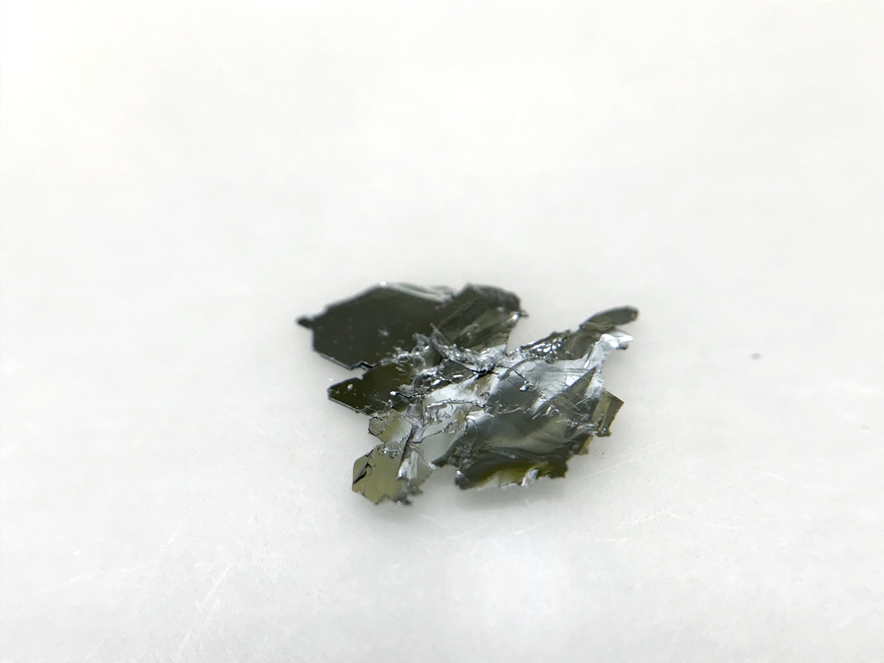
簡(jiǎn)要描述:100% environmentally stable metallic NbSe2 crystals: In the bulk form, niobium diselenide is metallic.
 產(chǎn)品型號(hào): 廠商性質(zhì):生產(chǎn)廠家更新時(shí)間:2024-06-03訪(fǎng) 問(wèn) 量:1070
相關(guān)文章
Related Articles詳細(xì)介紹
100% environmentally stable metallic NbSe2 crystals: In the bulk form, niobium diselenide is metallic. Similar to molybdenum disulfide, it has layered structure (lamellar) with weak interlayer coupling. NbSe2 displays metallic and superconducting behavior. Undergoes superconducting transition at low temperatures, exhibits CDW behavior. Unlike other sources, our NbSe2 crystals are grown by defect and impurity free flux zone technique (see the comparison between chemical vapor transport [CVT] below). Clean and defect free nature enabled researchers to observe clean superconductivity, phase transitions, and perform quantum transport measurements with confidence in the crystal.
If your research needs atomically flat NbSe2 samples for scanning tunneling microscopy (STM) measurements please contact us.
Properties of NbSe2 crystals by 2Dsemiconductors USA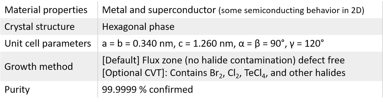
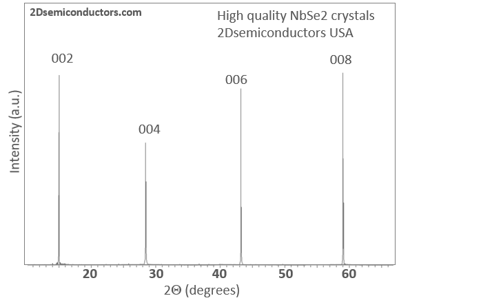
Growth method matters> Flux zone or CVT growth method? Contamination of halides and point defects in layered crystals are well known cause for their reduced electronic mobility, reduced anisotropic response, poor e-h recombination, low-PL emission, and lower optical absorption. Flux zone technique is a halide free technique used for synthesizing truly semiconductor grade vdW crystals. This method distinguishes itself from chemical vapor transport (CVT) technique in the following regard: CVT is a quick (~2 weeks) growth method but exhibits poor crystalline quality and the defect concentration reaches to 1E11 to 1E12 cm-2 range. In contrast, flux method takes long (~3 months) growth time, but ensures slow crystallization for perfect atomic structuring, and impurity free crystal growth with defect concentration as low as 1E9 - 1E10 cm-2. During check out just state which type of growth process is preferred. Unless otherwise stated, 2Dsemiconductors ships Flux zone crystals as a default choice.
產(chǎn)品咨詢(xún)
聯(lián)系我們
上海巨納科技有限公司 公司地址:上海市虹口區(qū)寶山路778號(hào)海倫國(guó)際大廈5樓 技術(shù)支持:化工儀器網(wǎng)掃一掃 更多精彩

微信二維碼

網(wǎng)站二維碼
微信掃一掃
 歡迎來(lái)到