13761090949

當(dāng)前位置:首頁 > 產(chǎn)品中心 > 二維材料 > 硫化物晶體 > MoWS2 二硫化鎢鉬晶體


簡要描述:Our MoWS2 alloys with the chemical formula MoxW(1-x)S2 crystals perfectly crystallize in 2H phase and come at different alloy ratios x.
 產(chǎn)品型號: 廠商性質(zhì):生產(chǎn)廠家更新時間:2024-06-03訪 問 量:848
相關(guān)文章
Related Articles詳細(xì)介紹
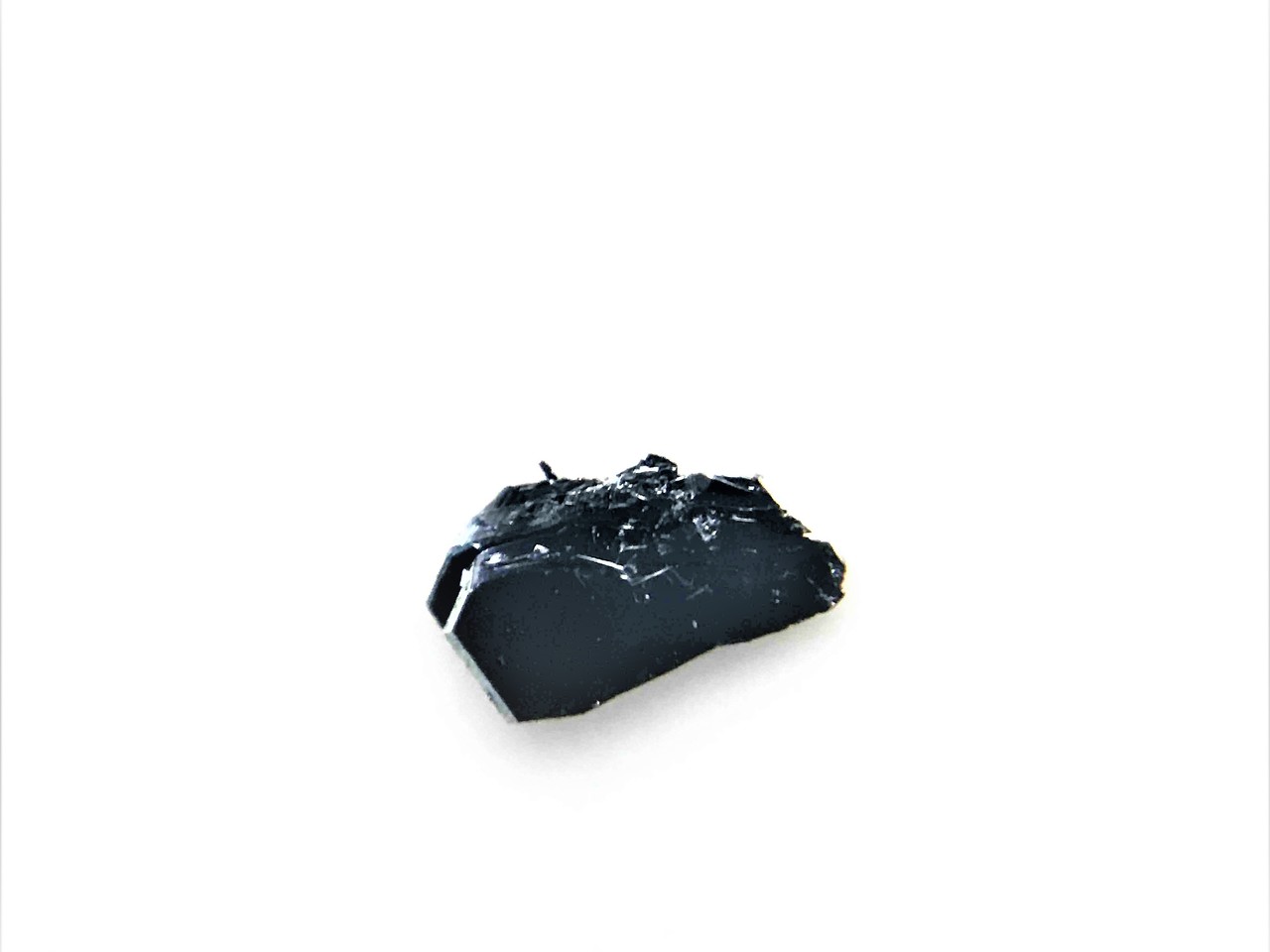
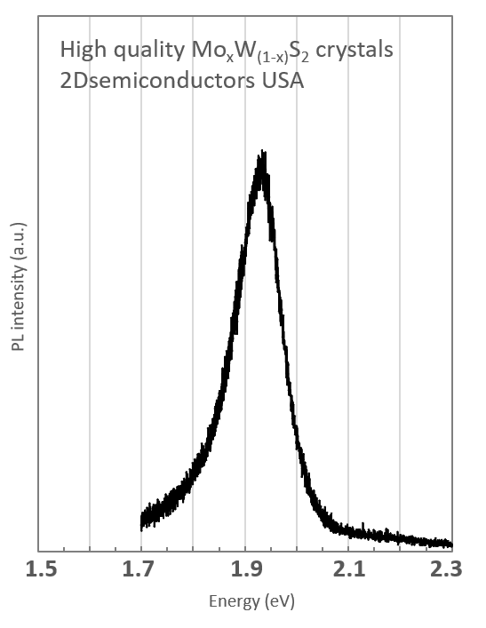
Our MoWS2 alloys with the chemical formula MoxW(1-x)S2 crystals perfectly crystallize in 2H phase and come at different alloy ratios x. Our crystals are grown using two different techniques through chemical vapor transport (CVT) or flux zone growth (see description of these two methods below) and their composition values were determined by XPS, SAED, and EDS measurements.. These crystals all possess extremely narrow PL bandwidths, display clean PL spectra, high carrier mobility, extremely clean and sharp XRD peaks, and negligible amount of defects (see published results as well as CVT vs. Flux based methods below). These crystals come with guaranteed alloying and valleytronic response, sharp PL, and good electronic response.
Important advantages of our crystals
1. Crystals come fully characterized using macro, micro, and nanoscale measurements (see below)
2. Thanks to our improved flux zone growth method, our crystals are homogeneously alloyed which means across the specimen you will only find one particular x composition.
3. No separation: Phase separation is commonly observed in 2D TMDCs alloys when cooling profiles are not controlled carefully. Our R&D team has worked over five (5) years to solely solve this problem.
Properties of layered MoWS2 alloys
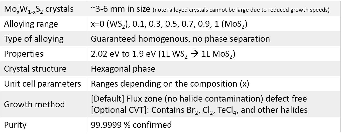
Growth method matters> Flux zone or CVT growth method? Contamination of halides and point defects in layered crystals are well known cause for their reduced electronic mobility, reduced anisotropic response, poor e-h recombination, low-PL emission, and lower optical absorption. Flux zone technique is a halide free technique used for synthesizing truly semiconductor grade vdW crystals. This method distinguishes itself from chemical vapor transport (CVT) technique in the following regard: CVT is a quick (~2 weeks) growth method but exhibits poor crystalline quality and the defect concentration reaches to 1E11 to 1E12 cm-2 range. In contrast, flux method takes long (~3 months) growth time, but ensures slow crystallization for perfect atomic structuring, and impurity free crystal growth with defect concentration as low as 1E9 - 1E10 cm-2. During check out just state which type of growth process is preferred. Unless otherwise stated, 2Dsemiconductors ships Flux zone crystals as a default choice.
產(chǎn)品咨詢
聯(lián)系我們
上海巨納科技有限公司 公司地址:上海市虹口區(qū)寶山路778號海倫國際大廈5樓 技術(shù)支持:化工儀器網(wǎng)掃一掃 更多精彩

微信二維碼

網(wǎng)站二維碼
 歡迎來到
歡迎來到