 歡迎來到上海巨納科技有限公司網站!歡迎來到上海巨納科技有限公司網站!
13761090949


相關文章
Related Articles詳細介紹
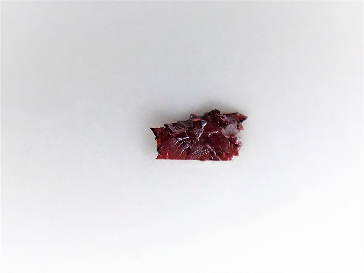
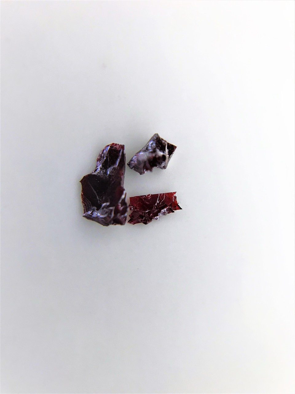
Gamma layered phase of In2S3 is a direct gap semiconductor with an optical band gap ranging from 2 eV - 3.25 eV. It's fundamental band gap nature (direct vs indirect) and its value have been much debaded in the field and remains open ended. In2S3 is particular attractive semiconductor for photoelectrochemical, solar cell, and photonic applications. Typical crystal sizes range in few-mm in size and each order contains 5-7 pieces of In2S3 crystals. The crystals appear layered but is harder to exfoliate compared to molybdenum disulfide. Thus, we recommend using highly adhesive tapes, ultrasonic exfoliation, or other methods to yield atomically thin sheets.
產品咨詢
聯系我們
上海巨納科技有限公司 公司地址:上海市虹口區寶山路778號海倫國際大廈5樓 技術支持:化工儀器網掃一掃 更多精彩

微信二維碼

網站二維碼
