13761090949

當(dāng)前位置:首頁 > 產(chǎn)品中心 > 二維材料 > 六方氮化硼 > 基于銅基的單層氮化硼薄膜(5*2.5cm)


簡(jiǎn)要描述:Single layer h-BN (Boron Nitride) film grown in copper foil.h-BN is an insulator with a direct band gap of 5.97 eV. Due to its strong covalent sp2 bonds in the plane, the in-plane mechanical strength
 產(chǎn)品型號(hào): 廠商性質(zhì):生產(chǎn)廠家更新時(shí)間:2024-06-03訪 問 量:1101
相關(guān)文章
Related Articles詳細(xì)介紹
Single layer h-BN (Boron Nitride) film grown in copper foil.
h-BN is an insulator with a direct band gap of 5.97 eV. Due to its strong covalent sp2 bonds in the plane, the in-plane mechanical strength and thermal conductivity of h-BN has been reported to be close to that of graphene. h-BN has an even higher chemical stability than graphene; it can be stable in air up to 1000 °C (in contrast, for graphene the corresponding temperature is 600 °C).
During Chemical Vapor Deposition, BN is grown on both sides of the copper foil
Specifications:
Close to complete coverage (90-95%), with some minor holes
Thickness of the copper foil is 20 microns
High crystalline quality, see SAD (Selected area [electron] diffraction) data
Quality is confirmed by TEM. TEM shows perfect hexagonal structure.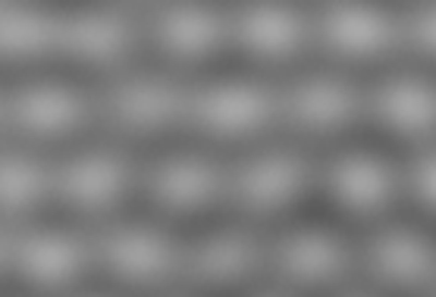
TEM image of perfect hexagonal structure

On SEM image (below), BN is seen as wrinkles on top of the copper foil.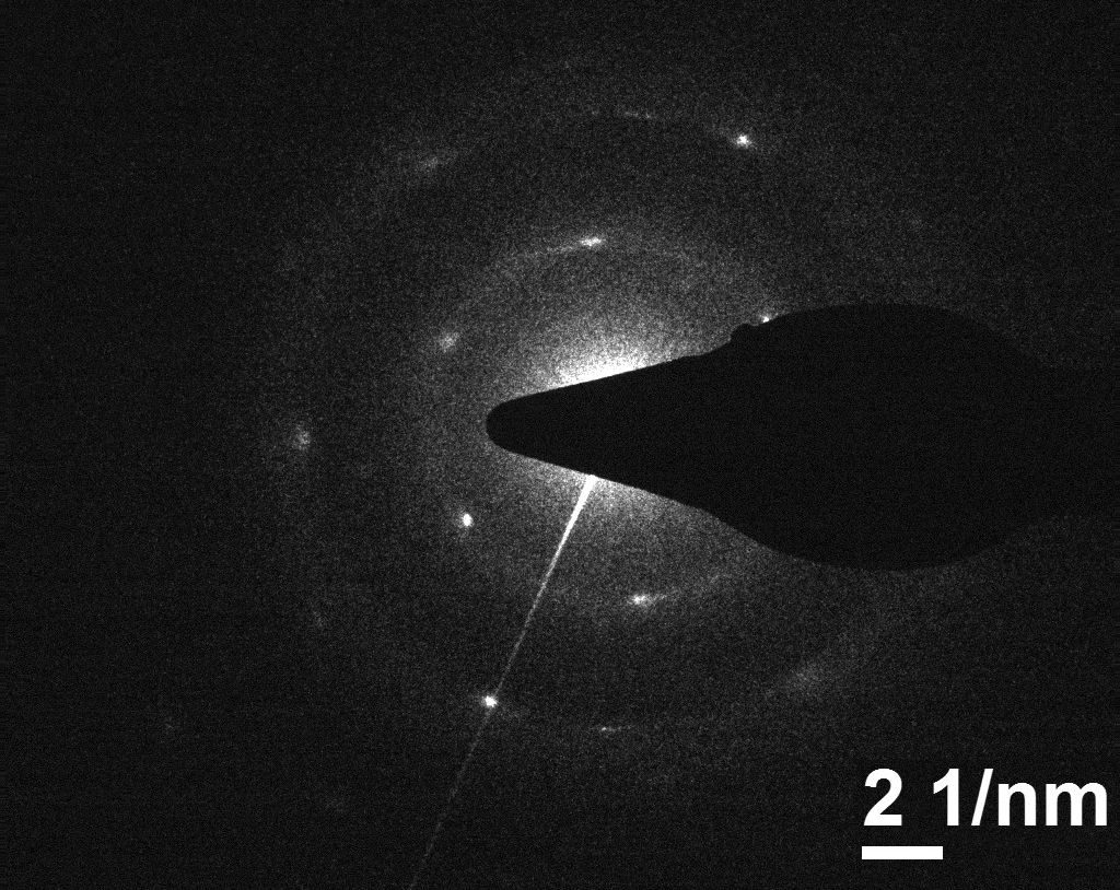
SAD data of h-BN
If transferred onto an SiO2 substrate, the BN film may be seen as a white film. However, it is difficult to recognize the BN film on copper using a microscope.
Absorbance data BN on copper
產(chǎn)品咨詢
聯(lián)系我們
上海巨納科技有限公司 公司地址:上海市虹口區(qū)寶山路778號(hào)海倫國際大廈5樓 技術(shù)支持:化工儀器網(wǎng)掃一掃 更多精彩

微信二維碼

網(wǎng)站二維碼
 歡迎來到
歡迎來到